89Sxx Development Board
89Sxx based SMS Controller

Click here for details
Nostalgic Crystal Radio
Click here for details
PC Based FM Radio
Click here to download schematic
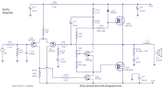
50 Watt MOSFET Audio Amplifier
Bi-Directional 2.4GHz RF Amplifier
100 Watt Inverter Circuit
Infrared Sensor (IR) Schematic Diagram
Infrared Sensor Schematic
LM 311- Comparator Controlled H-Bridge Motor Driving Circuit Diagram
H-Bridge Motor Control Circuit Using L298
100 Watt Inverter Circuit Diagram
Transmitter FM 45W
Tendency of catering: 220V ACFrequency of emission at FM: 88~108MHzForce of expense: max 45W (without the R3),Components & Their values.....
R1 15KW/2W R2 1KW/10W R3 1KW/10W (for biggest force in the exit you replace with short-circuit). C1 50pF trimmer C2 30pF trimmer C3 22pF/4KV C4, c6, c9 10nF/1KV C5, c7 1nF/1KV C8 100mF+100mF/450V (Double electrolytic) C9, c10 10nF RFC1, rfc2, rfc3 air Inductors: 15 coils diameter 8mm, from wire 1mm. T1 Transformer 220V/6V-1A T2 Transformer of configuration with being first 4 or 8W T3 Inductor with core ferrite (externally it resembles with small transformer but has a turn only). D1 BY127 rectifier Lamp 807 SYLV USA or EL34 or equivalent ANTENNA Simple dipole L/2. (L= wave length) S1 Main switch of catering. S2 Switch of catering of rise (him we close after zestacej' the thread). Most elements you can him find in a old back-white television with lamps.Regulations:
Source: http://www.electronics-lab.com
Stereo Fm Transmitter using BH1417 IC
Capacitors C18 and C19 are DC decoupling capacitors for the left and right channel inputs. Capacitors C1 and C17 are used to set the amount of pre-emphasis required and here with the used values it is 50uS. Capacitors C2 and C16 sets the roll-off point of the low pass filter. The crystal X1 is a 7.6MHz crystal which sets the oscillator’s frequency while capacitors C13 and C14 associated with are used for providing the appropriate loading. Resistors R8 to R11 are the pull-up resistors for the D0 to D3 (pins 15 to 18 of the IC) respectively. These pins can be held low by closing the corresponding switches. The RF oscillator of the IC is tuned using the components L1, C11, C12 and D1. Capacitor C11 prevents and DC voltage being applied to the varicap diode D1 and thereby prevents current flow into the inductor L1. More over it reduces the effects of changes in the capacitance of D1 on the pin 9. Capacitor C7 prevents any DC current from flowing into the inductor L1 from pin 9 of the IC. The composite output signal at pin 5 is applied to the junction of R6 and R7 though a network comprising of components C4, C5, C6 and R1. In the circuit pin 19 of the circuit is left unconnected, but an optional capacitor at this pin can be used to set the pilot level and phase. Any way such a capacitor is not at all a necessity here and the circuit will work perfectly even if the capacitor at pin 9 is omitted.
The composite output signal undergoes some attenuation while passing through this network and finally reaches the varicap diode D1. The carrier frequency is controlled using the PLL (phase lock loop) phase detector output pin (pin 7) and the components connected around it. The darlington transistor Q1 is driven by the output of the pin7 and the transistor applies a control voltage on the varicap diode through resistor R5, R6 and R7. Capacitor C10 works as a high frequency filter while R7 is meant for isolation. Resistor R4 and capacitor C9 connected in series between the collector and base of Q1 provides further filtering. Resistor R4 improves the response of the transistor to transient changes while capacitor C9 improves low frequency filtering. Capacitor C8 connected between collector and base of Q1 provides additional high frequency filtering. Resistor R3 serves as the collector load for the transistor Q1.
The modulated RF output is available at pin 11 and it is fed to the antenna through a filter network consisting of components L2, L3, C20, and C21. The job of this filter network is to remove harmonics. Resistors R12, R13 and R14 reduces the signal level to the antenna and as a result decreases the output power of the transmitter. Such a reduction is necessary to make the transmitter legal because in many countries transmitters that has an output power more than few milli watts (may change from nation to nation) are illegal. By omitting R12, R13, R14 and connecting the antenna directly to the junction of L2 and C21, the range can be increased, but do it at your own risk.
source:http://www.circuitstoday.com
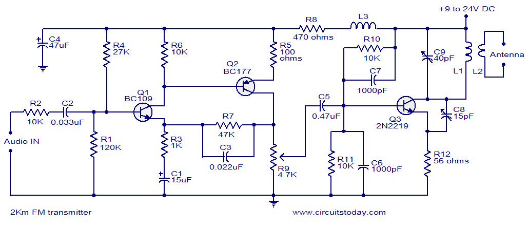
2 km FM transmitter
Description.
With a matching antenna, the FM transmitter circuit shown here can transmit signals up to a range of 2 kilo meters. The transistor Q1 and Q2 forms a classic high sensitive preamplifier stage. The audio signal to be transmitted is coupled to the base of Q1 through capacitor C2. R1, R3, R4, R6, R5 and R9 are the biasing resistors for the preamplifier stage comprising of Q1 and Q2. Transistor Q3 performs the collective job of oscillator, mixer and final power amplifier.C9 and L1 forms the tank circuit which is essential for creating oscillations. Inductor L2 couples the FM signal to the antenna.
With a matching antenna, the FM transmitter circuit shown here can transmit signals up to a range of 2 kilo meters. The transistor Q1 and Q2 forms a classic high sensitive preamplifier stage. The audio signal to be transmitted is coupled to the base of Q1 through capacitor C2. R1, R3, R4, R6, R5 and R9 are the biasing resistors for the preamplifier stage comprising of Q1 and Q2. Transistor Q3 performs the collective job of oscillator, mixer and final power amplifier.C9 and L1 forms the tank circuit which is essential for creating oscillations. Inductor L2 couples the FM signal to the antenna.
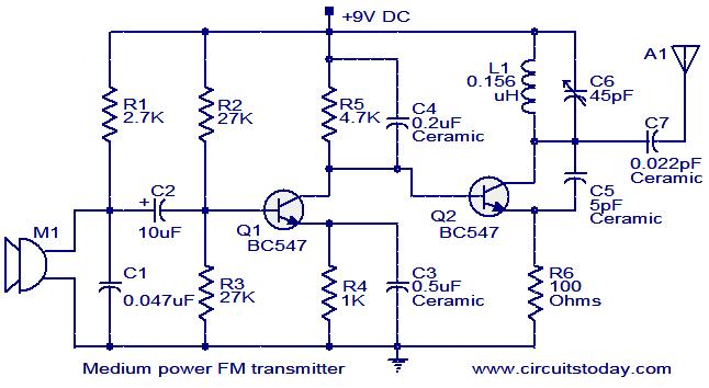
Medium power FM transmitter circuit
Description.
This is the circuit diagram of a moderate power FM transmitter circuit employing two transistors.The voice signals picked by the microphone will be amplified by the transistor Q1.The second transistor is wired as an oscillator operating in the FM band.The output of T1 is given to the base of T2.T2 performs the modulation also.The tank circuit comprising of components L1 and C6 determines the frequency of the signal, and can be varied by adjusting C6.The capacitor C7 couples the FM signal to the antenna.
Circuit diagram with Parts list.

more coming soon


No comments:
Post a Comment